
Wafer Handling Components
Precision CNC Machining for Wafer Handling Components
At AXALLOY, we understand that semiconductor equipment relies on flawless material transfer. A single microscopic defect, slight warpage, or surface irregularity in wafer handling components can lead to wafer damage, contamination, and costly equipment downtime.
We specialize in machining complex, high-value components from difficult alloys. Whether your engineering team is developing a prototype end effector or your procurement team needs a stable, low-volume production route for vacuum chucks and robotic arms, we provide the manufacturability feedback, process control, and documentation you need to eliminate supply chain risks.
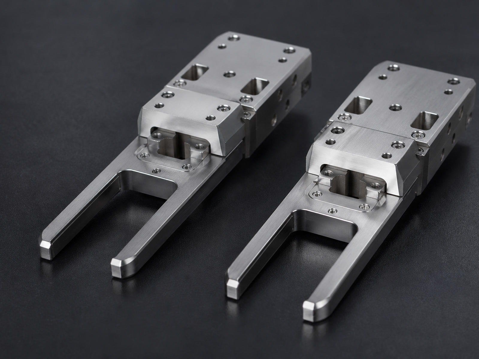
What You Gain When Partnering with AXALLOY
We focus on delivering tangible results for your engineering, quality, and procurement teams. Here is how our machining processes directly benefit your semiconductor applications:
Secure, Damage-Free Wafer Transfers
Wafer end effectors and robotic arms require extreme flatness and positional accuracy to prevent uneven stress on silicon wafers. By utilizing our 5-axis CNC milling and precision grinding capabilities, we achieve flatness down to 0.005 mm and positional tolerances to 0.010 mm. This ensures your components maintain perfect alignment during high-speed robotic movements, drastically reducing the risk of wafer slippage or breakage.
Cleanroom-Ready Surface Integrity
Particulate generation is the enemy of semiconductor manufacturing. We control our machining and finishing processes to deliver surface finishes down to Ra 0.2 μm via precision grinding, and Ra 0.8 μm through precision milling. This minimizes micro-burrs and porous surfaces, ensuring your components can be effectively cleaned, passivated, and integrated into vacuum or cleanroom environments without outgassing or shedding particles.
Faster Design Iteration for Engineering Teams
In the semiconductor industry, waiting on parts delays your entire equipment development schedule. We offer prototype lead times of 5–10 business days. This speed means your mechanical engineers can quickly validate new end effector geometries, test vacuum grip designs, and resolve design flaws weeks earlier than standard sourcing timelines allow.
Audit-Proof Quality and Traceability
Your quality and supplier management teams cannot accept undocumented parts. We provide comprehensive project-specific quality records. From Material Test Reports (MTR) confirming the exact grade of your titanium or stainless steel, to First Article Inspection (FAI) reports and full dimensional data verified by CMM, you receive the exact documentation required to pass your internal and customer audits.
Materials Suited for Wafer Processing Environments
Wafer handling components often operate in harsh environments involving high temperatures, corrosive gases, or extreme vacuums. We specialize in machining the difficult alloys required for these conditions:
Titanium Alloys (Grade 2, 5, 23)
Ideal for lightweight, low-inertia robotic arms and end effectors requiring high strength and low thermal expansion.
Stainless Steels (316L, 17-4 PH, 15-5 PH)
Highly stable materials for structural components, vacuum chucks, and susceptors requiring excellent corrosion resistance.
Nickel-Based Superalloys (Inconel 718/625, Hastelloy C-276)
Used for components exposed to high-temperature chemical vapor deposition (CVD) or etching processes.
Specialty Metals
Including aluminum alloys (commonly used for standard handling) and molybdenum for specific thermal requirements.
Material Selection Support
Choosing the right material is critical for wafer handling performance. Our engineers provide guidance on material selection based on your specific operating environment, thermal requirements, and weight constraints.
- Application-specific material recommendations
- Certified material sourcing with full traceability
- Alternative material options for cost optimization
- Surface treatment and passivation guidance
Technical Capabilities for Wafer Handling Components
Before we cut any material, our engineering team evaluates your part's geometry, tolerances, and surface requirements to define a stable manufacturing process. Below are our standard and precision capabilities.
| Parameter | Standard / Precision Capability |
|---|---|
| Supported Production Volume | 1–500 parts (Prototype to Low-Volume Production) |
| Prototype Lead Time | 5–10 business days |
| Standard Lead Time | 10–20 business days |
| Precision Dimensional Tolerance | ±0.005 mm |
| Position Tolerance | Down to 0.010 mm |
| Flatness | Down to 0.005 mm (Critical for vacuum chucks) |
| Concentricity / Roundness | Down to 0.008 mm / 0.005 mm |
| Precision Machined Finish | Ra 0.8 μm |
| Ground Surface Finish | Down to Ra 0.2 μm |
| Minimum Wall Thickness | 0.5 mm (Ideal for lightweight end effectors) |
| Minimum Machined Hole / Thread | Ø0.5 mm / M1.0 |
| 5-Axis Milling Envelope | Up to Ø500 × 400 mm |
| Precision Grinding Envelope | Up to 600 × 300 × 350 mm (Surface Grinding) |
| Wire EDM Cutting Accuracy | Down to ±0.005 mm (For narrow slots and sharp internal corners) |
Inspection and Quality Control
We know that for semiconductor equipment OEMs and Tier 1 suppliers, quality is not just a promise—it is verified data. Our temperature-controlled inspection room is equipped to validate the most complex geometries.
Inspection Equipment & Accuracy
- CMM Measuring Range: 700 × 1,000 × 600 mm (Accuracy up to 1.8 + L/300 μm)
- Optical Measurement Accuracy: ±0.002 mm
- Surface Roughness Range: Ra 0.05–40 μm
Available Quality Documentation
- Material Test Reports & Mill Test Certificates
- First Article Inspection Report (FAI)
- Full Dimensional Inspection Report & Ballooned Drawings
- Surface Roughness Reports
- Material and Lot Traceability Records
- Special Process Records (Heat treatment, passivation, coating)
Start Your Project with AXALLOY
If you are transferring a critical project from an unreliable supplier, or need a dependable manufacturing route for your next generation of wafer handling components, we are ready to evaluate your design.
How to get a precise quote:
Send us your complete 2D drawings (PDF, DWG) and 3D models (STEP, IGS, SLDPRT). Please include your defined materials, critical tolerances, expected quantities, and required quality documentation.
Our engineering team will review your files and provide actionable Design for Manufacturability (DFM) feedback along with a comprehensive pricing and lead-time proposal.
Submit Your RFQ TodayRequest a Quote
Tell us about your component requirements and material challenges.